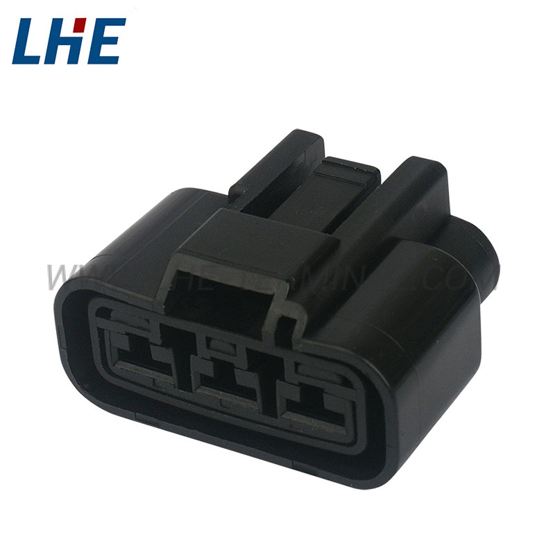
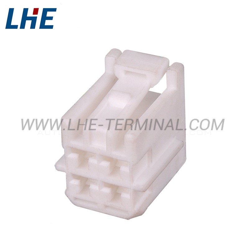
7225-2482 16 Position Female Crimp Terminal Housing

Original Part Number: 7225-2482

LHE Part Number: 215001620282

Number of Positions: 16

Contact Tab Size Series: 1.5

Size (MM): L:26 W:64 H:18.84

Seal or Unseal: Unseal

Overview:

LHE PN: 215001620282
Certification: TUV, IATF16949, ISO14001, ISO9001, CQC, UL, ROHS
MOQ: Most product not have MOQ, Small order can be accepted.
Sample service: Free Samples
Delivery Time: 3-5 Days
Quality Control All goods will be 100% inspected before dispatched
Payment: T/T, Western Union, MoneyGram, PayPal; 30% deposits; 70% balance before delivery.
Shipment: DHL/FedEx/TNT/UPS/EMS/Aramex/SF for samples, By Air or by Sea for batch goods; Airport/ Port receiving.

Enquiry Form


Corrosion trap
When the angle between the PCB leads is too small (acute angle), corrosion traps (Acid Trap) may be formed. These sharp-angled connections may remain in the corrosion solution during the corrosion stage of the circuit board, thereby removing more copper plating at the place, thereby forming stuck points or traps. In the later stage, the lead wire may be broken, resulting in an open circuit. Due to the use of photosensitive etching solutions in modern manufacturing processes, this corrosion trap phenomenon has been greatly reduced.
Tombstone device
When using the reflow process to solder some small surface mount devices, the device will form a single-ended warping phenomenon under the infiltration of solder, commonly known as “tombstone”. This phenomenon is usually caused by an asymmetrical routing pattern that causes uneven heat spread across the device pad. Tombstoning can be effectively mitigated with proper DFM checks.
Lead Width
When the current of the PCB leads exceeds 500mA, the first wire diameter of the PCB will appear to have insufficient capacity. With the usual thickness and width, the wires on the surface of the PCB pass more current than the wires inside the multilayer circuit board, because the surface leads can dissipate heat through air flow. The line width is also related to the thickness of the copper foil on the layer. Most PCB manufacturers allow you to choose copper foil with different thickness from 0.5 oz/sq.ft to 2.5 oz/sq.ft.